Start with the student’s own question
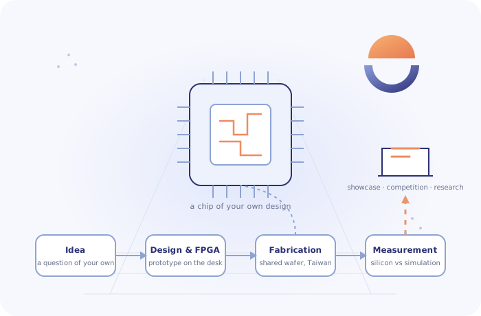
Most young people who build robots or electronics assemble a standard microcontroller and write code for it. The chip inside is somebody else’s. YSRP starts one level deeper. A student brings a question of their own—can a purpose-built circuit cut the latency and energy of a robot’s sensor processing under stated conditions; can a wake-up detector run for years on a coin cell; can a tiny circuit make each device uniquely identifiable; can a sensor front end make an environmental project more reliable—and the programme helps them answer it with a chip they design themselves.
Because the question is the student’s own, so is the work that follows: the design decisions, the trade-offs, the measurements and the story. That is what showcases, competition judges and university readers respond to, and it is why every YSRP project begins with the question rather than with a kit.
Design, verify, prototype, fabricate, measure
YSRP is a twelve-week programme followed by fabrication. Weeks one to four build the foundations: how logic becomes hardware, how to describe a design, how to test it. Weeks five to eight are spent on the student’s own project, running on an FPGA so that it works on the desk long before any silicon exists. Weeks nine to twelve cover verification, documentation and the engineering notebook. In week thirteen the design is submitted for fabrication on a shared wafer; the packaged chip and its development board arrive about six to nine months later, and the student measures their silicon against their simulation.
Each student works with an engineer-mentor from the group’s Taipei team in one-to-one sessions, alongside a small weekly group. The mentor reviews, questions and signs off; the student designs. See the week-by-week programme and calendar ↗
To see what a finished project looks like before you begin, read the worked example: Tick-to-Signal, a chip that turns a stream of market prices into a trading signal in one clock cycle ↗. Every student’s project differs from it; the example shows the method, the measurements and what a family can expect.
AI assistance, without expensive design software
Professional chip design depends on commercial design-automation (EDA) licences that cost hundreds of thousands of dollars a year—one reason it has never been part of education. YSRP students do not buy any of it. Every design is completed in the YSRP Studio—Magellan Global’s own AI-assisted design-automation platform for young designers, developed with MTRI. The Studio runs in a browser and carries the whole flow: design entry (block-based logic for beginners, hardware description for those ready for it), simulation, verification checks, FPGA programming, the pre-fabrication checks the shuttle requires, a fabrication tracker, and measurement reports when the silicon returns. Underneath, it is built on proven open-source tools, which is why it can be offered at a fraction of the cost of commercial software and to any school or region.
Inside the Studio, an AI design assistant explains, checks and asks why, rather than designing for the student. Every exchange is kept with the project and becomes part of the disclosure statement that competitions and journals require, so the student can show exactly what was their own work. The engineering notebook, the design document and the public project page are generated from the Studio’s own records.
The Studio is deliberately built in stages. The first cohorts use the browser edition described above. The next stage is a visual, game-like design mode in which a young person can assemble and test a chip of their own as naturally as building a world in a sandbox game, and a schools edition that a teacher can run without a semiconductor background. The aim is simple: the cost and difficulty of designing a chip should stop being the reason young people never do it.
Taiwan: where the chip is made, and the people who make it
Fabrication uses multi-project wafers on mature 130–180 nm processes, through partner shuttle services in the United States and Germany, with packaging, test boards and measurement handled by the group’s engineering team in Taipei. Every cohort is booked on two independent fabrication routes so that a delay on one does not stop a student’s chip.
Taiwan is where the modern semiconductor industry is concentrated, and understanding how chips are actually made—how a shuttle is scheduled, what packaging and test involve, how design services, foundries and assembly plants divide the work—is part of what students take away. The optional Taipei silicon week brings students to that ecosystem in person: visits to fabrication and packaging facilities, measurement sessions in the lab, and time with the engineers who reviewed their designs. In the age of AI, chips are the physical foundation of everything else; YSRP lets young people see that foundation for themselves.
What students take away
We describe outcomes at three levels of certainty, and we keep the distinction on every page and in every agreement.
What every student receives. A chip of their own design, with its development board; a working FPGA prototype; an engineering notebook and design documentation; a disclosure statement covering AI and mentor involvement; a public project page; a certificate and a place in the cohort showcase; and continued access to the YSRP Studio for the next design. Together these make a finished project in the form that science fairs, robotics competitions and student journals expect, and the student can go on to enter them—with the programme’s support through the outcomes pack, or independently.
What the outcomes pack supports. Entry through the student’s regional ISEF-affiliated science fair, or to an open-hardware robotics competition such as WRO Future Innovators or RoboCupJunior Rescue Maze, and submission of the project to a peer-reviewed student journal or an open-hardware conference. We publish each cohort’s participation and acceptance figures once they exist.
The highest goals. For a project that has become real research, the goals we help families aim at are the top awards of the established international research competitions—Regeneron ISEF above all, with Regeneron STS, EUCYS, the Yau Science Award and Davidson Fellows where the student is eligible—and, for the rare mature project, a professional paper at a venue such as FPGA, DAC or ICCAD. No youth chip competition carries the weight of an IMO or IOI gold, and we do not pretend otherwise; these are the recognised targets, and each depends on the student. The highest goals, eligibility and the routes to them ↗
Where the finished project can go next
A completed YSRP project is not the end of the road; it is the entry ticket. With a working chip, measured data, an engineering notebook and a design document, a student is in a position to take the work on to the competitions, programmes and venues below. Eligibility depends on age, where the student studies and each organiser’s rules, and we map the route with each family before dates are fixed. Full details, eligibility and achievement levels ↗
| Route | Where the project can go | Typical timing |
|---|---|---|
| Research competitions | The regional ISEF-affiliated science fair (TISF, SSEF, the Hong Kong competition, JSEC, US state fairs, CWSF, Jugend forscht and others), leading to Regeneron ISEF; Regeneron STS for US-eligible final-year students; EUCYS by national nomination; the Yau Science Award; Davidson Fellows; the Thermo Fisher Junior Innovators Challenge and 3M Young Scientist Challenge for US middle-school students. | The fair season after the silicon returns |
| Robotics competitions | WRO Future Innovators (any controller, from age 8), WRO Future Engineers and RoboCupJunior Rescue Maze, where the student’s own hardware can be central; FIRST leagues as a sensing or co-processing module. | The next national season |
| Publication | A first paper in a peer-reviewed student journal such as the Journal of Emerging Investigators, or a talk at an open-hardware conference; for the rare mature project, a professional venue such as FPGA, DAC, ICCAD or ICRA. | Three to nine months after the silicon returns |
| Within the group | The Taipei silicon week; the next design on the YSRP Studio; later, introductions to GSRP-related internships and the group’s talent network for outstanding participants; co-authorship of MTRI’s research on the programme where a student’s contribution warrants it. | From the following cohort onwards |
How deep the work goes
“My child made a chip” can mean anything from completing a template to a measured piece of research, so we say exactly which level the programme reaches. Every student designs and debugs their own function (not a kit), poses a question and measures their design against alternatives, and receives their own fabricated silicon to test against simulation. The mentor reviews and signs off; the AI assistant explains, checks and records; the student designs, decides and writes. MTRI studies the programme as it runs and publishes the results either way. The four levels, who does what, the research programme and the platform ↗
Why a chip of their own matters
Most students never enter a research competition at all. Of those who do, almost every engineering project is built on a standard microcontroller, so it competes with thousands of others built the same way. A project that answers its question with a chip the student designed, and that compares a bought controller, an FPGA implementation and the student’s own silicon on measured latency, energy or accuracy, is rare enough to be remembered—and it carries evidence that no kit can provide. Judges at the major fairs reward exactly that: a clear question, alternatives considered, real tests, and a student who understands and can defend every decision.
The same holds in robotics. Most leagues fix the robot’s main controller, so the student’s chip appears there as a sensor or co-processing module that measurably improves the robot; competitions such as WRO Future Innovators allow any controller and reward an original solution to a real problem. Either way, the student can explain every step from idea to silicon, because they took every step. That understanding of how things are made is what remains when the chip is in a drawer—and it is what shapes how a generation of young people will think about the hardware underneath AI.
How journeys become opportunity
Magellan Global’s name recalls a voyage, and the story behind the name describes a pattern: people who crossed into an unfamiliar world brought back an understanding of how it worked, and that understanding became opportunity. The group’s Mobility Capital framework studies the same pattern in adults who work across borders.
YSRP applies it to a young person’s first journey. The crossing is not only geographic. A student who can write code crosses into hardware, into manufacturing, into the laboratories and factories of Taiwan, and onto an international stage. They come back with knowledge of how things are made, with judgement formed by real trade-offs and real measurements, and with opportunities that follow from a result of their own. Knowledge, judgement and opportunity are the three components of Mobility Capital; a first chip is where many young people will begin to accumulate them.
From YSRP to GSRP: one pathway
The group runs two programmes on the same principle. GSRP develops enterprise-nominated successors and key people through AI capability, genuine work and international experience. YSRP does the same for students aged 12 to 17, at the scale of a first project. Families planning a successor’s development can begin years earlier; outstanding YSRP participants may later be introduced to GSRP-related internships and to the group’s talent network. Research on both programmes is carried by MTRI, and family education planning is supported through AJPE.
Formats, and how to join
YSRP is offered as a twelve-week programme delivered online with small weekly groups and one-to-one mentoring, in English with Mandarin-language groups for the first cohorts in Singapore, Taiwan and Hong Kong. The outcomes pack adds publication and competition support after the chip returns. The Taipei silicon week is an optional in-person week. A schools edition supports a teacher-led cohort with mentor support and a fabrication allocation. Cohorts open twice a year and are timed to the fabrication schedule; places in each cohort are limited by mentor capacity.
Under-18 participants enrol through a parent or guardian account. We collect the minimum information needed to deliver the programme, keep AI assistant logs for the student’s own disclosure and for the group’s research only with consent, and arrange any travel for the Taipei week with WG Global’s specialists. Fees, eligibility and other questions ↗
What we do not promise
YSRP does not guarantee awards, publication or admission to any school or university. Competitions and journals require that a project be the student’s own work with mentoring disclosed, and the programme is built to meet that standard rather than to work around it. Fabrication on shared wafers can be delayed; if both booked routes fail, the silicon portion of the fee is refunded or the design is placed on the next run, at the family’s choice. Fees, dates and formats are confirmed for each cohort before enrolment.