YSRP · Twelve-week programme
From a student’s own question to a fabricated chip, with mentors and an AI design assistant.
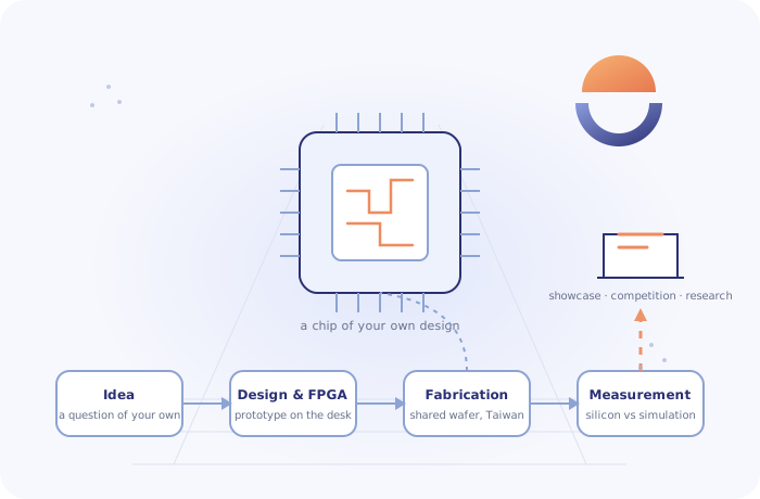
What we help you do
- 01
Choose and scope a question of the student’s own, then design the logic that answers it on the YSRP Studio.
- 02
Prove the design on an FPGA, record decisions in an engineering notebook, and prepare it for fabrication with a mentor’s review.
- 03
Submit on two booked fabrication routes, receive the packaged chip, and measure it against simulation.
What the engagement produces
- A working FPGA prototype and the student’s own fabricated chip with its development board—designed entirely on the YSRP Studio, Magellan Global’s AI-assisted design-automation platform, with no commercial EDA licence to buy.
- Design document, engineering notebook and a disclosure statement generated from the Studio’s records.
- A public project page, a certificate, a place in the cohort showcase, and a finished project ready to go on to the regional ISEF-affiliated fair, an open-hardware robotics competition or a first publication.
How it works
Enrol in a cohort timed to the fabrication schedule; receive the development board.
Twelve weeks of group sessions and one-to-one mentoring with the group’s Taipei engineers, working on the YSRP Studio.
Fabrication, return of silicon, measurement; optional outcomes pack and Taipei silicon week.
Your questions, answered.
Is prior electronics experience needed?
No. Basic programming experience is enough; the first weeks build the hardware foundations.
Can the student keep working on the design afterwards?
Yes. The student keeps the copyright, retains access to the studio, and can submit improved designs to later runs.
Make it relevant to you.
Tell us the student’s age, interests and location. We will confirm the next cohort.